This page details the motivations, high-level theory of operation, and installation instructions for my modification PCB that improves the quality of the video in Super Famicom and Super Nintendo 3-chip consoles.
Most Super Famicom and Super Nintendo consoles, when compared to the last "1-Chip" and "Mini" revisions, have curiously blurry video. It is not as simple as a low-pass filter, but instead one that produces different rates of change in video levels based upon the characteristics of the transition. Hard edged transitions can appear quite sharp, while mid-levels may have slow transitions resulting in a blur or "shadow" effect. This has been discussed to death so I will avoid reiterating too much here.
My simple PCB is being sold at 家電のケンちゃん in Akihabara, Tokyo; plans are underway to sell it in the United States.
To view an image at full-size, right click it and navigate to the source URL.

I discovered some experiments done by shmups forum user yoshiyukiblade, and wanted to immediately build a circuit to test it. The amp it called for is in a rather small package so making a PCB for testing seemed like the right choice.
Without repeating information needlessly from the linked thread, in short we're feeding back in some high-frequency content in the video to try and counter what appears to be the effects of parasitic capacitance within S-PPU2, alongside the DAC's impedance varying based upon what pixel transition is occuring.
One goal was to try to make this mod uninvasive - a simple board to attach to the underside in place of a few transistors, that would pump improved video through all of the original RGB paths afterwards. I mean all of them! Not only is the RGB improved, but the S-video and even Composite / NTSC video receive minor improvements. In addition, the encoder acts as another buffer. The performance of the filter cannot be affected by incorrect termination or cable construction (though other issues that may cause remain unabated).
As the voltage is different, as are the characteristics of whatever comes afterwards in the video path, the feedback capacitor values were adjusted accordingly. To do so, I grabbed my TI filter handbook and began solving for the value that would hit the 9MHz knee I was targeting grabbed an assortment of capacitors and tried various values until I struck a balance of sharpness and (invisibility of) ringing.
The original DAC has some flaws, particularly a high amount of ringing on some transitions (seemingly when one of the higher bits changes, the second MSB?) and this kit will not change that.
From SHVC board to board, or revision to revision, there is a certain amount of noise present in a stock console. In addition to random noise, other common sources of noise include:
These problems are generally issues that stem from the way the board has been laid out and traces routed, or inadequate filtration of the main power rail (5V). You can mitigate the second one pretty easily by installing additional bypass capacitors of a higher capacity than was common at that time (e.g. a 10uF X7R capacitor here and there). Stick them underneath the PPU chips, and throw one on the main 7805 LDO's output too, while you're at it. That will probably get rid of the line in the middle of the screen you get from the DRAM refresh, as a bonus.
Version 1.2 supports the first revision of the Super Famicom / SNES PCB, marked SHVC-CPU. Compared to 1.0, this version has a dedicated voltage regulator providing the 4.75V PPU DAC supply, as well as a better layout that greatly simplifies installation. It is no longer necessary to lift one leg of the PPU or solder a diode to the top side; everything is done from the bottom side now.
Before installing the PCB, the underside of the Super Famicom board must undergo some revisions. On the underside, right below the cartridge slot, is the first part of the RGB amp / buffer circuit. Remove the following from the PCB:

If available, I suggest using copper braid or another solution to remove as much solder as possible from the pads. This will level the surface and make a clean installation of the board possible.
Through isolation of one via on the underside, it is possible to supply a different voltage to the PPU DAC pin as with revision 1.0, but without bothering the PPU pin directly.
Locate the highlighted via between R12 and R7, and use a knife or dremel to remove the copper connecting it to the surrounding 5V supply.

Once the cutting is complete, I suggest using a multimeter to verify that there is no continuity between the via and the 5V supply (a test point can be the "O" pin of the 7805 voltage regulator, near the top-right of the PCB on the underside).
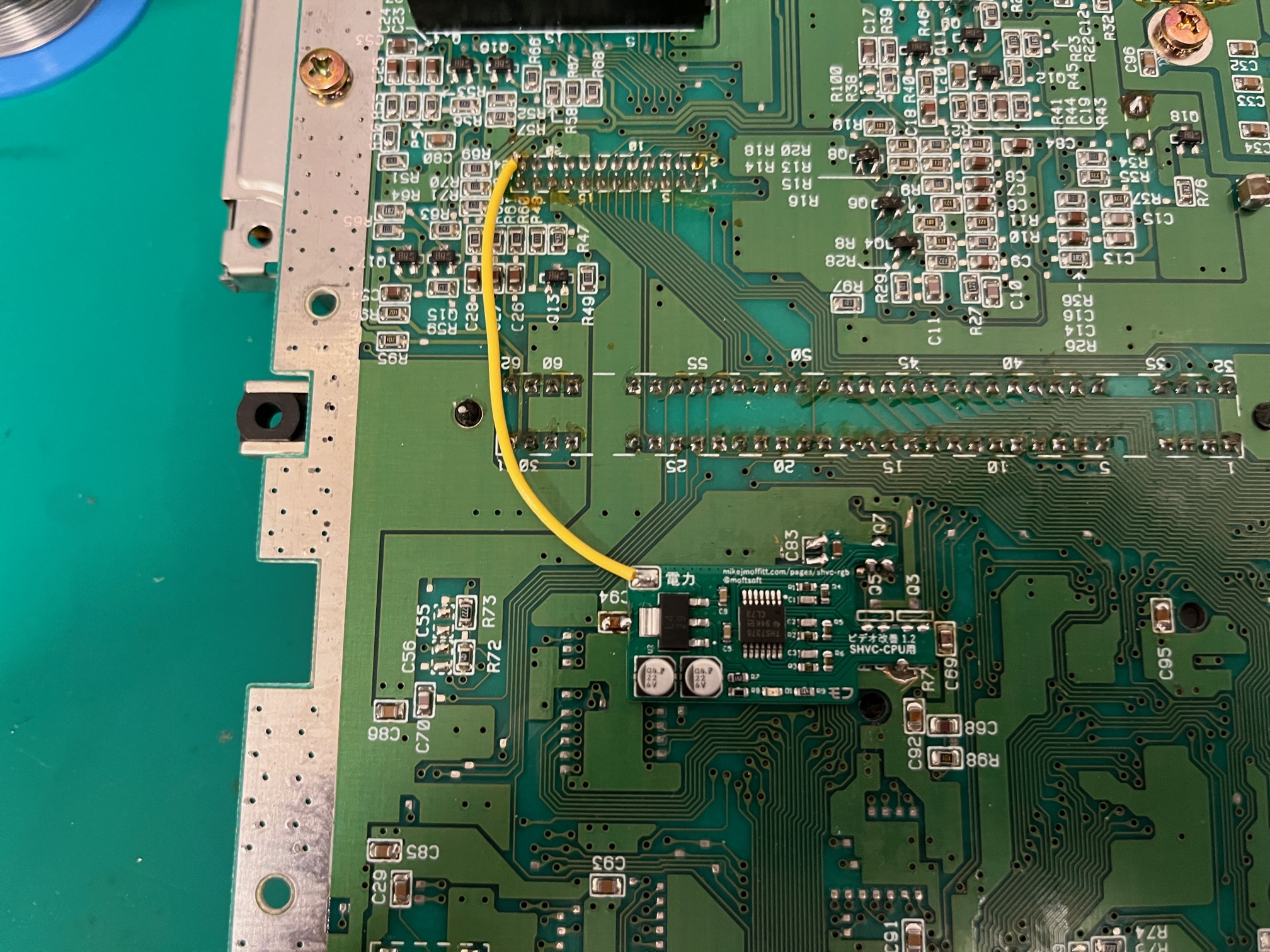
Finally, the PCB may be soldered. Line the PCB up as in this photograph, and solder the castellated edges to the corresponding pads. The leftmost side of the board is soldered to the right side of C94. Near the top of the kit PCB are two points that solder to C83, but the distance is a little high so a small solder blob will become necessary. I apologize for this small mechanical aberration. Don't worry about having removed C83, as the capacitor on the PCB replaces it.
Be careful when doing the connection to the via that we just isolated before, as it is a little bit tricky. If the video is blank, then this pin is not making a connection, or there is a short circuit. If there is a shrot circuit on the DAC line, the orange LED will not illuminate. If you failed to isolate the pin and it still has the original 5V, the video will be a little blown out, and if left that way it may damage the voltage regulator.
Once the PCB is installed, one wire must be run to power the voltage regulator. Solder a wire from the APU module connector pin 24 to the top-left solder pad on the kit PCB.
When you are done, things should look like this:
I suggest heading over to the modification section to make a small change that can reduce interference from other signals on the board.
The present version (v1.0) supports only the first revision of the Super Famicom / SNES PCB, marked SHVC-CPU. This model is identifiable by the presence of a separate sound module in the back-right corner. The "GPM" revision can also be used, but as the layout has changed it would require six additional wires. I'll be addressing it down the line, so for now I recommend just sticking to the original SHVC-CPU revision.
The kit includes the small modification PCB, three wires, and a BAT54C SOT-23 diode. Please ensure these parts are all present.
Disassemble the Super Famicom / SNES fully. We will need to access the underside of the PCB as well as the top, so shielding must be removed from the motherboard during the installation. It can be installed again after the work is complete.
The voltage of the video levels must be slightly lowered to avoid clipping when being amplified by the kit. To do this, we will lower the voltage of S-PPU2's DAC voltage supply. A very small change is needed, so dropping the voltage using only a diode is acceptable.
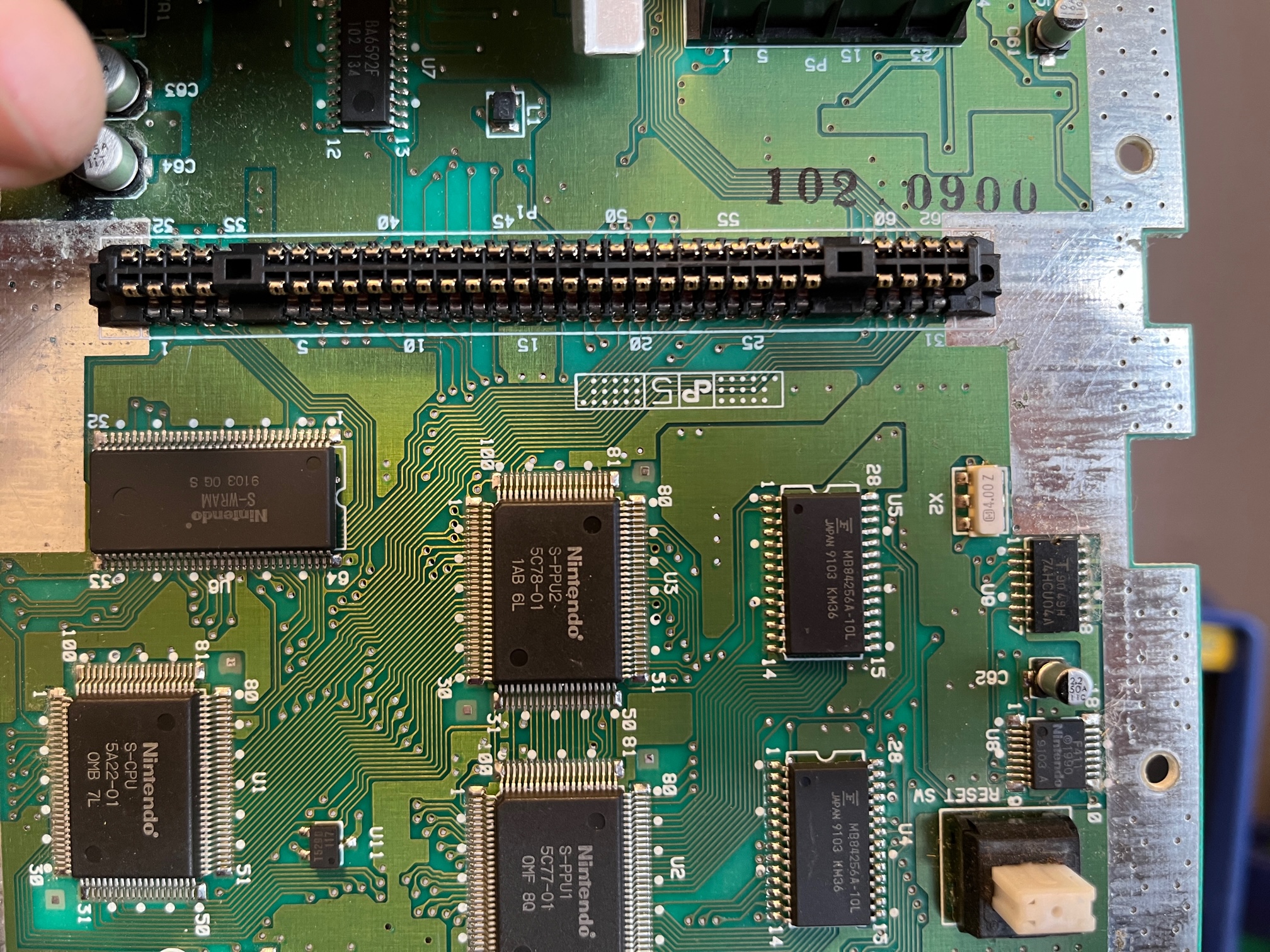
This photo shows where S-PPU2 is present, and the location of relevant pins and signals.
Desolder S-PPU2’s AVVC pin (pin 94) and gently lift it using a hobby knife, tweezers, or whatever tool feels comfortable. This pin is fragile, so be gentle. Optionally, you may insulate the area below the pin using kapton tape to make further work easier.
Afterwards, scrape a small amount of solder resist off of the nearby 5V supply trace, and solder the two adjacent legs of the diode to this plane. Finally, run a wire between the previously lifted AVCC pin and the remaining single pin of the diode. The picture below shows what this looks like when installed.

After doing this, hook up power, video, and a cartridge, and test the system. It should still work as before, if not with a slightly darker image. If it does not work, check your soldering and verify that there are no shorts.
Turn the main PCB over so we may focus on the backside. Below the cartridge slot is the location shown in the picture below. The RGB preamp transistors have been highlighted.

Three transistors (Q3, Q5, Q7) must be removed. Gently desolder them and clean the pads using a solder wick so that the area is relatively flat.

Place the kit PCB as shown in the picture, and make sure to align the castellated edges with the lower pads of the transistors you removed. Once it is in place, carefully solder the PCB to the pads as shown. There are four pads on the lower side, including one that is on the corner, and two pads on the upper side.

Finally, using the two remaining wires, solder a wire to the VCC pad in the top-right of the kit PCB to the capacitor shown in the picture below. Afterwards, do the same for the GND pad.

Now, you may power on the system and verify that the video still works, and has been improved. Afterwards, reassemble it. You are done.
Below are some before and after shots. These were taken poorly using a phone (and a new one with a camera I simply do not like) so please excuse the moire patterns and odd angles. The setup shown is an LG C1 TV (configured as a PC input to remove odd edge enhancements and color compression) with an OSSC, in Line4X mode, with the generic profile.
For Super Mario World, take note of the transition on the left side of the letters in the title from black to the main color. The yellow letter shows the difference particularly strongly. Notice also how the bush on the left loses its "shadow" after the kit has been installed.


Mother 2's before image of the menu is a screaming indignment of the original design. It has been significantly improved in the after image.


Again with Mother 2, the simple design of the environment of this game shows it off quite well.

Teenage Mutant Ninja Turtles 4: Turtles In Time

Super Mario World

KiKi KaiKai: Nazo no Kuro Manto

KiKi KaiKai: Nazo no Kuro Manto (On CRT)

I have become a little more aware of interference picked up by the video lines as they travel from one end of the Super Famicom board to another. In the case of the SHVC-CPU revision, particularly the red channel seems susceptible to this. It is a little defeating to admit it, as it goes against one of the original goals of this mod board, but you may get better results by cutting the three traces that carry RGB up towards the video encoder, and replacing them with wires of your own installation.
To do so, make the cuts marked in orange in this diagram. Then, run wires from the pads marked in red, green, and blue. This is best done after the kit PCB is installed.

These two pictures show the before and after when just the red was rewired in this fashion; the vertical interference marks all but vanished.

